

KnowHow
Free Technical Resources
How to add a register map into an OVM scoreboard
Doulos, April 2010
Constrained randomization is a great way to find bugs quickly and thoroughly explore a design's state space, quickly reaching 100% design coverage. OVM's built-in randomization, hierarchial stimulus (sequences), and testbench architecture are designed from the ground-up to accomodate a constrained-random stimulus verification environment.
When coming from a directed testing background, it is very tempting to incorporate self-checks directly into the hierarical sequences—and indeed, there may be cases where this is necessary. However, the best approach is to use monitors on each interface, which send observed transactions to a scoreboard where the behavior is then checked for correctness. This frees up the stimulus to be more flexible, reusable, and of course, random. Test cases simply become the controller that guides the random stimulus while the testbench itself handles all the necessary checking.
Since a design is controlled by its state elements, and these elements are configured through its registers, the only way to know what a design will do is to either directly tap into the RTL's storage elements or accurately model the design registers in the scoreboard. Probing registers directly into a design's RTL may not be so easy to do, especially if the register bits are scattered throughout the design or do not exist at all (for example, some registers are write only for kicking-off behavior but the values are never stored). Likewise, hierarchical references into the design have other issues like maintaining correct paths across design changes or reusability.
Instead, a better approach is to create an accurate shadow model of the design's registers, which the scoreboard can use to model and determine the correct behavior of the design. Registers come in many shapes, sizes, and behaviors like read-write, read-only, write-only, read-clear, reset-upon-write, shared-address registers, indirect registers, and many more. Also, a verification environment should have a quick and easy back-door access to the registers without going through the interface bus-protocol in order to achieve faster simulation performance and simplify behavior modeling.
The easiest way to model the registers is to start with a basic, parameterizable class object and extend it to accomodate the various members and behaviors. While this is not particularly difficult to do, modeling registers and all their behaviors can become quite tedious and time-consuming—contrary to the goal of verification, which is finding bugs, not writing code! Instead, a better approach is to use one of the contributed register packages at OVM World.
There are two register packages donated to the OVM World: one from Mentor and one from Cadence. Both offer different approaches and features worth considering. Have a look at this post if you need help deciding on which one to select.
For this tutorial, we will be using Cadence's "Register and Memory Package", which they call RGM. This package has many great features like:
While this package can be used for defining memories, we will only look at the register subset.
For this tutorial, we will use a simple SPI (Serial Peripheral Interface) design found on the OpenCores website here. This design has a Wishbone system interface and transfers SPI data in full duplex mode.
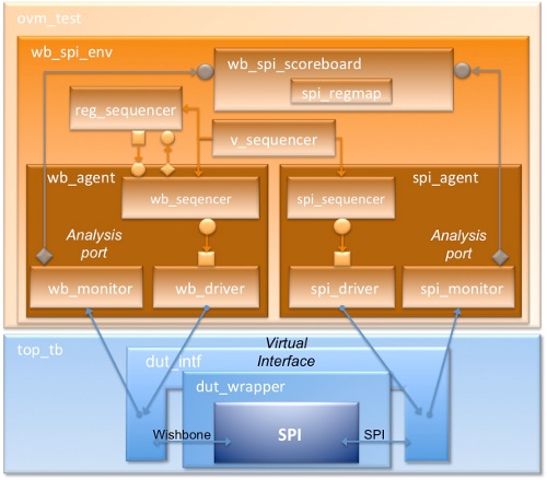
The verification environment is constructed in two parts—one verification agent for the Wishbone (WB) interface and one for the SPI interface. A virtual sequencer is used to coordinate transfers between the Wishbone and SPI domains, and the interface monitors snoop transactions and send them over to a scoreboard for correct functional checking.
Inside the scoreboard, the register map will be used for checking the design. Since the SPI design simply converts data from parallel to serial and vice versa, no functional or behavior modeling is really required—only checking the transactions values against the shadow register map. We will also incorporate the RGM register sequencer into the environment for easy register testing. The environment will look like this:
To follow along with the examples used in this tutorial, we invite you to download the source code for this environment here.
We can use the RGM package to create our register map in 5 easy steps:
The first step to building the register map is identifying all the registers, their fields, and attributes. For the OpenCores SPI design, the functional specification specifies the following registers:
| Name | Address | Width | Access | Reset Value | Description |
|---|---|---|---|---|---|
| RX0 | 0x0 | 32 | R | 0x00000000 | Data receive register 0 |
| RX1 | 0x4 | 32 | R | 0x00000000 | Data receive register 1 |
| RX2 | 0x8 | 32 | R | 0x00000000 | Data receive register 2 |
| RX3 | 0xc | 32 | R | 0x00000000 | Data receive register 3 |
| TX0 | 0x0 | 32 | R/W | 0x00000000 | Data transmit register 0 |
| TX1 | 0x4 | 32 | R/W | 0x00000000 | Data transmit register 1 |
| TX2 | 0x8 | 32 | R/W | 0x00000000 | Data transmit register 2 |
| TX3 | 0xc | 32 | R/W | 0x00000000 | Data transmit register 3 |
| CTRL | 0x10 | 32 | R/W | 0x00000000 | Control and status register |
| DIVIDER | 0x14 | 32 | R/W | 0x0000FFFF | Clock divider register |
| SS | 0x18 | 32 | R/W | 0x00000000 | Slave select register |
These registers have the following field layouts:
| Bit # | 31:0 |
| Access | R |
| Name | RXn |
| Bit # | 31:0 |
| Access | R |
| Name | TXn |
| Bit # | 31:14 | 13 | 12 | 11 | 10 | 9 | 8 | 7 | 6:0 |
| Access | R | R/W | R/W | R/W | R/W | R/W | R/W | R | R/W |
| Name | Reserved | AS/td> | IE | LSB | TX_NEG | RX_NEG | GO_BSY | Reserved | CHAR_LEN |
| Bit # | 31:16 | 15:0 |
| Access | R | R/W |
| Name | Reserved | DIVIDER |
| Bit # | 31:8 | 7:0 |
| Access | R | R/W |
| Name | Reserved | SS |
The next step is to capture these register specifications in a SPIRIT-XML file and use the RGM package's IP-XACT parser to automatically generate the SystemVerilog code for the registers and the register map.
Starting with the first register, we could describe it in XML using the following attributes:
| RX/TX Register 0 | |
|---|---|
| name | rxtx0 |
| description | data receive/transmit register 0 |
| addressOffset | 0x0 |
| size | 32 |
| access | read-write |
| reset | 0x0 |
This would be written in SPIRIT-XML format like this:
<spirit:register>
   <spirit:name>rxtx0</spirit:name>
   <spirit:description>Data receive/transmit register 0</spirit:description>
   <spirit:addressOffset>0x0</spirit:addressOffset>
   <spirit:size>32</spirit:size>
   <spirit:access>read-write</spirit:access>
   <spirit:reset>
      <spirit:value>0x00000000</spirit:value>
      <spirit:mask>0xffffffff</spirit:mask>
   </spirit:reset>
</spirit:register>
Cadence has also extended the SPIRIT syntax with additional vendor extensions. While not required, they offer some very useful features like specifying register coverage options, soft reset values, comparison masks, indirect register addressing, hierarchical reference paths for backdoor access, random constraints, and more.
With this design, the RX and TX registers share the same address. RGM supports shared addressing for registers, but that is not needed in this case because RX and TX actually do share the same register storage elements. Therefore, only one register will be described for each address. By default, the automatic generation will create a new class definition for every register, but RX[0-3] and TX[0-3] all have the same structure so only one class definition is really needed. We can use a vendor extension to make sure only one class definition is created—the type extension:
<spirit:register>
   ...
   <spirit:vendorExtensions>
      <vendorExtensions:type>spi_rxtx_register</vendorExtensions:type>
   </spirit:vendorExtensions>
</spirit:register>
Here we have specified that the RX/TX0 register will use the class definition called spi_rxtx_register.
Now what about more complicated registers with multiple fields with different access types such as the SPI Control/Status register? For this, we can use the optional field tag along with the name, bitOffset, bitWidth, and access tags. Here is how it would look:
<spirit:register>
   <spirit:name>ctrl</spirit:name>
   <spirit:description>Control and status register</spirit:description>
   <spirit:addressOffset>0x10</spirit:addressOffset>
   <spirit:size>32</spirit:size>
   <spirit:reset>
      <spirit:value>0x00000000</spirit:value>
      <spirit:mask>0x00003f7f</spirit:mask>
   </spirit:reset>
   <spirit:field>
      <spirit:name>reserved</spirit:name>
      <spirit:bitOffset>14</spirit:bitOffset>
      <spirit:bitWidth>18</spirit:bitWidth>
      <spirit:access>read-write</spirit:access>
   </spirit:field>
   <spirit:field>
      <spirit:name>as</spirit:name>
      <spirit:bitOffset>13</spirit:bitOffset>
      <spirit:bitWidth>1</spirit:bitWidth>
      <spirit:access>read-write</spirit:access>
   </spirit:field>
   <spirit:field>
      <spirit:name>ie</spirit:name>
      <spirit:bitOffset>12</spirit:bitOffset>
      <spirit:bitWidth>1</spirit:bitWidth>
      <spirit:access>read-write</spirit:access>
   </spirit:field>
   <spirit:field>
      <spirit:name>lsb</spirit:name>
      <spirit:bitOffset>11</spirit:bitOffset>
      <spirit:bitWidth>1</spirit:bitWidth>
      <spirit:access>read-write</spirit:access>
   </spirit:field>
   <spirit:field>
      <spirit:name>tx_neg</spirit:name>
      <spirit:bitOffset>10</spirit:bitOffset>
      <spirit:bitWidth>1</spirit:bitWidth>
      <spirit:access>read-write</spirit:access>
   </spirit:field>
   <spirit:field>
      <spirit:name>rx_neg</spirit:name>
      <spirit:bitOffset>9</spirit:bitOffset>
      <spirit:bitWidth>1</spirit:bitWidth>
      <spirit:access>read-write</spirit:access>
   </spirit:field>
   <spirit:field>
      <spirit:name>go_bsy</spirit:name>
      <spirit:bitOffset>8</spirit:bitOffset>
      <spirit:bitWidth>1</spirit:bitWidth>
      <spirit:access>read-write</spirit:access>
   </spirit:field>
   <spirit:field>
      <spirit:name>char_len</spirit:name>
      <spirit:bitOffset>0</spirit:bitOffset>
      <spirit:bitWidth>7</spirit:bitWidth>
      <spirit:access>read-write</spirit:access>
   </spirit:field>
</spirit:register>
We can use some vendor extensions for this register as well. Since this is the control register, we can specify random constraints so that the built-in random sequences do not try to set bits that are not allowed. For example, the GO_BSY flag should not be set to 1 unless the SPI is ready to transmit so we could constraint it to 0. We could also constraint other fields like setting LSB field to 1 so the LSB is always sent first, or the IE bit set so an interrupt is automatically generated upon completion. These constraints would be specified like this:
<spirit:register>
   <spirit:name>ctrl</spirit:name>
   ...
   <spirit:vendorExtensions>
      <vendorExtensions:constraint>  no_go_c { value.go_bsy == 0; }
      </vendorExtensions:constraint>
      <vendorExtensions:constraint>  ie_c { value.ie == 1; }
      </vendorExtensions:constraint>
      <vendorExtensions:constraint>  as_c { value.as == 1; }
      </vendorExtensions:constraint>
      <vendorExtensions:constraint>  lsb_c { value.lsb == 1; }
      </vendorExtensions:constraint>
      <vendorExtensions:constraint>  txneg_c { value.tx_neg == 1; }
      </vendorExtensions:constraint>
      <vendorExtensions:constraint>  rxneg_c { value.rx_neg == 1; }
      </vendorExtensions:constraint>
   </spirit:vendorExtensions>
</spirit:register>
The constraint syntax is just simple SystemVerilog constraints. When the generator creates the register definitions, these constraints will be directly inserted into the class definition. The value member is a packed structure with the raw register field values. The individual fields are named according the field definitions in the XML above.
Defining the registers is only half of the XML definition. The SPIRIT-XML format also allows us to specify different address and memory mappings. For this example, we can keep it simple and just define one. Our address map will start at address 0x0 and cover 0x2c addresses (each register being 32-bits). The rest of our XML file will look like this:
<?xml version="1.0"?>
<spirit:component xmlns:spirit="...">
   <spirit:vendor>cadence</spirit:vendor>
   <spirit:library>spi</spirit:library>
   <spirit:name>spi_regmap</spirit:name>
   <spirit:version>1</spirit:version>
   <spirit:memoryMaps>
      <spirit:memoryMap>
         <spirit:name>spi</spirit:name>
         <spirit:addressBlock>
            <spirit:name>regs</spirit:name>
            <spirit:baseAddress>0x0</spirit:baseAddress>
            <spirit:range>0x2c</spirit:range>
            <spirit:width>32</spirit:width>

            <spirit:register>
               <!-- ... field definitions go here ... -->
            </spirit:register>

            <!-- ... register definitions go here ... -->

         </spirit:addressBlock>
      </spirit:memoryMap>
   </spirit:memoryMaps>
</spirit:component>
For a detailed description of the supported SPIRIT-XML syntax, please refer to the RGM User Guide. All the examples described here can be downloaded in our sample OVM SPI tutorial.
An easier way to describe all the registers in XML is to download Eclipse and use the RGM Eclipse plug-in. This will allow you to define your registers graphically and easily change the XML file.
With the XML defined, we can now generate the register map using the RGM IP-XACT parser:
%  java -jar $OVM_RGM/builder/ipxact/ovmrgm_ipxact2sv_parser.jar \
	-i spi_regmap.xml -o spi_regmap.sv -ov -ve internal
This generates the following output:
Simple register definition ...// Data receive/transmit register 0
class spi_rxtx_register extends ovm_rgm_sfld_register #(32);
`ovm_object_utils(spi_rxtx_register)
function new(input string name="unnamed-spi_rxtx_register");
super.new(name);
set_reset_value(ovm_rgm_hard_reset, 32'h0, 32'hffffffff);
set_reset_value(ovm_rgm_soft_reset, 32'h0, 32'h0);
endfunction
endclass : spi_rxtx_register
Register definition with fields ...
// Control and status register
class ctrl_type extends ovm_rgm_sized_register #(32);

  typedef struct packed {
    logic [17:0] rsv1;
    logic as;
    logic ie;
    logic lsb;
    logic tx_neg;
    logic rx_neg;
    logic go_bsy;
    logic rsv;
    logic [6:0] char_len;
  } pkd_flds_s;

  `ovm_object_utils(ctrl_type)

  `ovm_rgm_fld_utils_begin(pkd_flds_s)
    `ovm_rgm_fld_int(0, rsv1, REG_RD_RSVD, REG_NO_WR, 14, 18, "")
    `ovm_rgm_fld_int(1, as, REG_RD, REG_WR, 13, 1, "")
    `ovm_rgm_fld_int(2, ie, REG_RD, REG_WR, 12, 1, "")
    `ovm_rgm_fld_int(3, lsb, REG_RD, REG_WR, 11, 1, "")
    `ovm_rgm_fld_int(4, tx_neg, REG_RD, REG_WR, 10, 1, "")
    `ovm_rgm_fld_int(5, rx_neg, REG_RD, REG_WR, 9, 1, "")
    `ovm_rgm_fld_int(6, go_bsy, REG_RD, REG_WR, 8, 1, "")
    `ovm_rgm_fld_int(7, rsv, REG_RD_RSVD, REG_NO_WR, 7, 1, "")
    `ovm_rgm_fld_int(8, char_len, REG_RD, REG_WR, 0, 7, "")
  `ovm_rgm_fld_utils_end

  constraint no_go_c { value.go_bsy == 0; }
  constraint ie_c { value.ie == 1; }
  constraint as_c { value.as == 1; }
  constraint lsb_c { value.lsb == 1; }
  constraint txneg_c { value.tx_neg == 1; }
  constraint rxneg_c { value.rx_neg == 1; }

  covergroup compare_and_update_cg;
    ...
  endgroup

  ...
endclass : ctrl_type
Register file ...
//////////////////////////////////////////////////////////////////////////////
// Reg_file definition
//////////////////////////////////////////////////////////////////////////////
class regs_type extends ovm_rgm_register_file;

  rand spi_rxtx_register rxtx0;
  rand spi_rxtx_register rxtx1;
  rand spi_rxtx_register rxtx2;
  rand spi_rxtx_register rxtx3;
  rand ctrl_type ctrl;
  rand divider_type divider;
  rand ss_type ss;

  `ovm_object_utils(regs_type)

  function new(input string name="unnamed-regs");
    super.new(name);
    set_size(`OVM_RGM_AWIDTH'h2c);
    rxtx0 = spi_rxtx_register::type_id::create("rxtx0");
    add_register(`OVM_RGM_AWIDTH'h0, rxtx0, "rxtx0");
    rxtx1 = spi_rxtx_register::type_id::create("rxtx1");
    add_register(`OVM_RGM_AWIDTH'h4, rxtx1, "rxtx1");
    rxtx2 = spi_rxtx_register::type_id::create("rxtx2");
    add_register(`OVM_RGM_AWIDTH'h8, rxtx2, "rxtx2");
    rxtx3 = spi_rxtx_register::type_id::create("rxtx3");
    add_register(`OVM_RGM_AWIDTH'hc, rxtx3, "rxtx3");
    ctrl = ctrl_type::type_id::create("ctrl");
    add_register(`OVM_RGM_AWIDTH'h10, ctrl, "ctrl");
    divider = divider_type::type_id::create("divider");
    add_register(`OVM_RGM_AWIDTH'h14, divider, "divider");
    ss = ss_type::type_id::create("ss");
    add_register(`OVM_RGM_AWIDTH'h18, ss, "ss");
  endfunction
endclass : regs_type
Address map ...
//////////////////////////////////////////////////////////////////////////////
// Address_map definition
//////////////////////////////////////////////////////////////////////////////
class spi_type extends  ovm_rgm_address_map;

  rand regs_type regs;

  `ovm_object_utils(spi_type)

  function new(input string name="unnamed-spi");
    super.new(name);
    set_size(`OVM_RGM_AWIDTH'h10000);
    regs = regs_type::type_id::create("regs");
    add_register_file(`OVM_RGM_AWIDTH'h0, regs, "regs");
  endfunction
endclass : spi_type
Register database ...
//////////////////////////////////////////////////////////////////////////////
// rdb definition
//////////////////////////////////////////////////////////////////////////////
class spi_regmap extends ovm_rgm_db;

  rand spi_type spi;

  `ovm_component_utils(spi_regmap)

  function new(string name = "unnamed-rgm_rdb", ovm_component parent);
    super.new(name,parent);
  endfunction : new

  virtual function void build();
    super.build();
    // Create the address map
    spi = spi_type::type_id::create("spi", this);
    add_addr_map(spi);
  endfunction : build
endclass : spi_regmap
Wow! All that code from a few XML statements! For a detailed description of the different RGM classes and macros, please have a look at the RGM User Guide.
Revisiting our testbench diagram, notice that our register map will live inside of the scoreboard. It could exist as a separate component in the testbench, but it is easiest to insert it directly inside the scoreboard where it will be used.
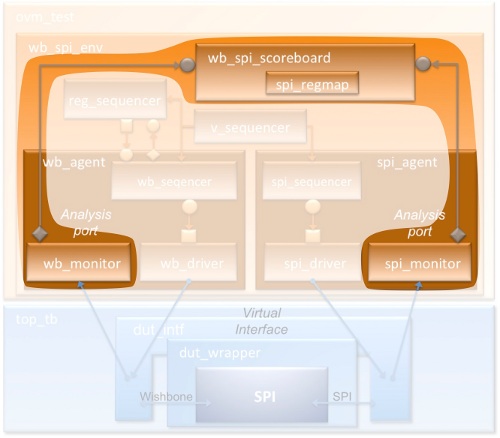
Also notice that analysis ports are connected from the Wishbone and SPI monitors to the scoreboard exports. These exports must have a corresponding write() method. The write() method will receive the monitor's transactions and either update the register map or check and compare the value against what is in the registers.
One issue that arises when using multiple analysis exports is that they all use the same write() method. Normally, this is not an issue if the same transaction type is used for each export, but in this case the transaction objects differ. The way around this problem is to use the`ovm_analysis_imp_decl( _suffix ) macro. This macro creates a wrapper class called ovm_analysis_imp_suffix#() that expects the user to define a method called write_suffix(). We can add these exports into our scoreboard along with the register map like this:
`ovm_analysis_imp_decl(_wb)
`ovm_analysis_imp_decl(_spi)

class wb_spi_scoreboard extends ovm_scoreboard;

   spi_regmap   m_regmap;

   ovm_analysis_imp_wb  #( wb_trans,  wb_spi_scoreboard ) wb_ap;
   ovm_analysis_imp_spi #( spi_trans, wb_spi_scoreboard ) spi_ap;

   function void build();
        super.build();

        // Create the TLM connections
        wb_ap  = new( "wb_ap",  this );
        spi_ap = new( "spi_ap", this );

        // Create the register map using factory method
        m_regmap = spi_regmap::type_id::create( "m_regmap", this );

   endfunction : build

   ...				// Constructor, etc.

endclass : wb_spi_scoreboard
Once the register map is instantiated in the scoreboard along with the analysis exports, we can update and compare incoming transactions with the values in the scoreboard.
Since the Wishbone interface reads and writes directly to the SPI registers, it is easiest to start with it. First, inside our scoreboard we will define the write_wb() method expected by ovm_analysis_imp_wb#():
function void write_wb( wb_trans t );
   ...
endfunction
Inside write_wb(), we need to decide what to do with the transaction. We have 3 types in this environment— RESET, RX (read), and TX(write). We will use the register map's built-in method get_reg_by_addr(), specifying the transaction's address, to obtain a reference to the object that refers to the target register:
function void write_wb( wb_trans t );
   ovm_rgm_register_base  dut_reg;
   dut_reg = m_regmap.spi.get_reg_by_addr( t.addr, 0 );
   ...
endfunction
With a reference to the register, we can now process the transaction. If the transaction is of type RESET, then we will perform a hard reset on the entire register map using the built-in reset() method. If the transaction is a write (TX), then we need to only update the register but not compare it. For a read (RX), we need to first compare it with the value in our register map and then update it with what we read from the design under test. We can implement our scoreboard like this:
class wb_spi_scoreboard extends ovm_scoreboard;
   ...
   function void write_wb( wb_trans t );

      // Get the register from the register map
      ovm_rgm_register_base dut_reg;
      dut_reg = m_regmap.spi.get_reg_by_addr( t.addr, 0 );

      // If a reset transaction, then reset the register map
      if ( t.kind == RESET ) begin
	 ovm_report_info( "WB SCOREBOARD", "Resetting the register map" );
	 m_regmap.spi.reset(ovm_rgm_hard_reset);
	 return;
      end

      // If a write, then update the shadow register map
      if ( t.kind == TX )
	 dut_reg.update_bv( 0, t.data, 0 );

      else
	 // Check that the data transferred is correct.  An error is issued
	 // if the value doesn't agree with the register shadow value.
	 assert( dut_reg.compare_and_update_bv( 0, t.data, 0 ))
   		ovm_report_error( "WB SCOREBOARD",
   				  "WB read mismatched with shadow register" );
   endfunction : write_wb
endclass : wb_spi_scoreboard
For our reset behavior, the reset() method accepts 2 arguments: ovm_rgm_hard_reset (="HARD") and ovm_rgm_soft_reset(="SOFT"). The driver asserts the external reset signal so we specify a hard reset.
The update_bv() method receives a value to update the register, collects coverage, and calls the pre- and post-access methods, which allow modification of the register value before the update or comparison takes place (e.g., masking off particular bits). The first argument is the offset into the register (typically 0), the next is the data value to update, the third argument when set to 0 means to write to all available bytes, and the fourth argument specifies the register mask, which when omitted specifies to not mask any bits. The compare_and_update_bv() works similarly to update_bv(), but also performs the comparison with the register and reports an error if there is a mismatch.
The SPI interface transfers between 1 to 128 bits of data so the SPI transactions have a larger data member than the Wishbone transactions, and data is simultaneously sent and received. Both the sent and received data needs to be checked, but only the relevant bits as specified by the CHAR_LEN field of the CTRL register. The monitor tallies the number of bits sent across the interface and reports it to the scoreboard. This tally is first checked against the register map's CTRL register, and then the data checked with the appropriate RX/TX registers:
class wb_spi_scoreboard extends ovm_scoreboard;
   ...
   function void write_spi( spi_trans t );
      int numbits;
      bit [127:0] mask;

      //------------------------------------------------------------------------
      // First, make sure that the control value sent by the monitor agrees with
      // the value in the control register.
      //------------------------------------------------------------------------
      void'( m_regmap.spi.regs.ctrl.compare_and_update_bv( 0, t.ctrl, 0,
      	     {7{1'b1}}));

      //------------------------------------------------------------------------
      // Create a mask for the bits to check.
      //------------------------------------------------------------------------
      numbits = t.ctrl.char_len ? t.ctrl.char_len : 128;
      for ( int i = 0; i < numbits; i++)
   	mask[i] = 1;

      //------------------------------------------------------------------------
      // RX Data - Mask off unused bits and check what was received
      //------------------------------------------------------------------------
      void'( m_regmap.spi.regs.rxtx0.compare_and_update_bv( 0,
      	     t.data_rx[31:0], 0, mask[31:0] ));

      if ( numbits > 32 )
	 void'( m_regmap.spi.regs.rxtx1.compare_and_update_bv( 0,
	        t.data_rx[63:32], 0, mask[63:32] ));
      if ( numbits > 64 )
	 void'( m_regmap.spi.regs.rxtx2.compare_and_update_bv( 0,
		t.data_rx[95:64], 0, mask[95:64] ));
      if ( numbits > 96 )
	 void'( m_regmap.spi.regs.rxtx3.compare_and_update_bv( 0,
		t.data_rx[127:96], 0, mask[127:96] ));

      //------------------------------------------------------------------------
      // TX Data - Mask off unused bits and check what was transmitted
      //------------------------------------------------------------------------
      void'( m_regmap.spi.regs.rxtx0.update_bv( 0, t.data_tx[31:0], 0,
	     mask[31:0]));

      if ( numbits > 32 )
	 void'( m_regmap.spi.regs.rxtx1.update_bv( 0, t.data_tx[63:32], 0,
	       mask[63:32] ));
      if ( numbits > 64 )
	 void'( m_regmap.spi.regs.rxtx2.update_bv( 0, t.data_tx[95:64], 0,
	        mask[95:64] ));
      if ( numbits > 96 )
	 void'( m_regmap.spi.regs.rxtx3.update_bv( 0, t.data_tx[127:96], 0,
	        mask[127:96] ));

   endfunction : write_spi
endclass : wb_spi_scoreboard
Unlike the write_wb() method above where we access registers using get_reg_by_addr() since we only know the address, we can access the RX/TX registers directly using a hierarchical reference because we know which registers to check.
With the write_wb() and write_spi() methods defined, the scoreboard is ready to start checking—nothing else is required! The RGM package adds the extra bonus of recording coverage every time the register map is updated.
For the full source code of the examples used in this tutorial, we invite you to download our example OVM SPI environment here. In exchange, we will ask you to enter some personal details. To read about how we use your details, click here. On the registration form, you will be asked whether you want us to send you further information concerning other Doulos products and services in the subject area concerned.
Next: Part 2 - Incorporating the RGM Built-in Test